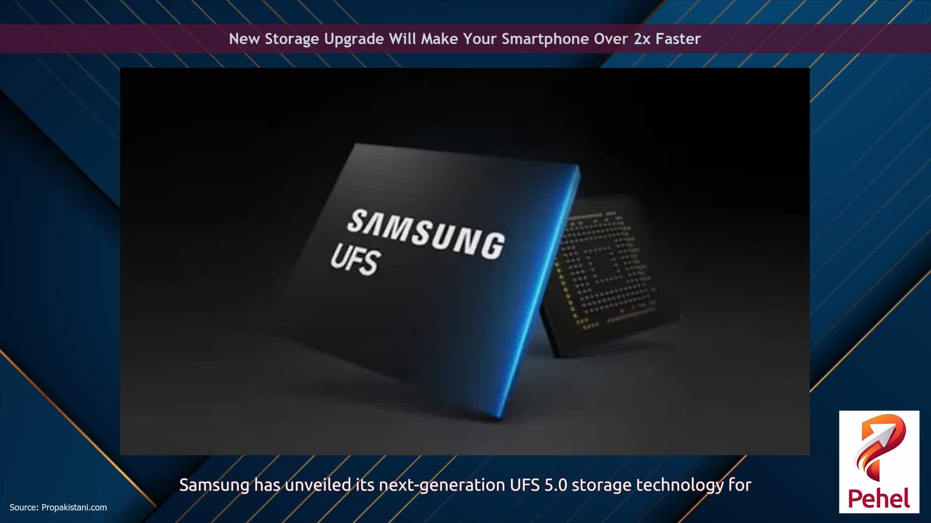
Samsung has revealed its roadmap for next-generation SSD technology that could dramatically increase storage capacity by stacking up to 1,000 layers of NAND flash memory.
The company says its new design could allow future SSDs to hold up to four times more data than current models, paving the way for consumer drives with capacities as high as 32TB.
The plans were outlined during the VLSI Symposium 2026, where Samsung explained how it intends to overcome the engineering challenges involved in building extremely tall NAND flash chips.
Rather than creating a single 1,000-layer chip, the company plans to bond two separate 450- to 500-layer NAND stacks together using a technology called Cell-Multi Bonding (CMB).
Samsung says demand for high-capacity SSDs is increasing rapidly, particularly as artificial intelligence, data centers, and enterprise workloads require more storage.
The company is accelerating its NAND development roadmap, with 420-layer NAND planned by 2029 and more than 560 layers expected by 2030. Beyond that, Samsung aims to surpass 1,000 layers early in the next decade.
Building NAND chips with hundreds of layers presents several manufacturing difficulties. One of the biggest issues is wafer warping, where the chip bends during production, making it harder to manufacture accurately.
Samsung says it has addressed this problem with a new “Upper Chuck” design that improves wafer stability during production. The company has also developed advanced overlay correction technology to reduce alignment errors when stacking large numbers of memory layers.
These improvements are intended to make ultra-high-layer NAND manufacturing more practical while lowering production challenges.
Instead of producing one massive NAND structure, Samsung’s approach combines two separate 450-layer memory stacks into a single package using Cell-Multi Bonding.
According to technology analyst Dr. Ian Cutress, this design could significantly increase SSD capacities. For example, an 8TB QLC SSD using today’s technology could potentially expand to as much as 32TB using Samsung’s future 1,000-layer architecture.
Samsung is not alone in the race to develop higher-density NAND memory.
Currently, SK Hynix leads the industry after becoming the first company to commercialize 321-layer NAND technology. The company is also developing 400-layer NAND using its own Hybrid Bonding manufacturing process, while Samsung is pursuing Vertical Bonding technologies for future products.
Meanwhile, Chinese memory manufacturer YMTC is rapidly expanding its NAND business. The company already produces 232-layer and 294-layer NAND chips and is investing heavily in new manufacturing facilities to increase production capacity as global demand for storage continues to rise.
Samsung’s 900- to 1,000-layer NAND technology remains in the prototype stage, with commercial products expected around 2030.
Before then, the company plans to introduce NAND chips with more than 400 layers over the next several years, gradually moving toward its long-term goal of delivering SSDs with significantly higher storage capacities than those available today.
Get the latest tech news, telecom insights, and product launches wherever you prefer.
Add ProPakistani to Preferred Sources and see more of our stories in Google Search and Top Stories.
Shares